VCC in DRAM - Integrated Circuits - - An Online Book - |
||||||||
| Integrated Circuits http://www.globalsino.com/ICs/ | ||||||||
| ================================================================================= | ||||||||
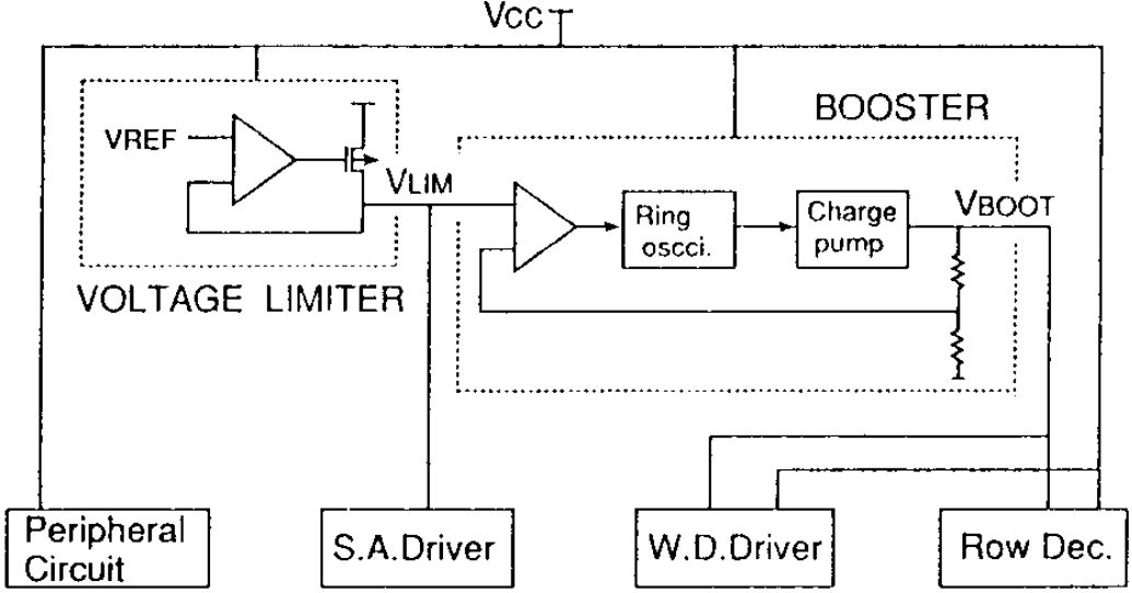
Figure 4962a shows the schematics of a typical power supply of DRAM. There are three voltage levels:
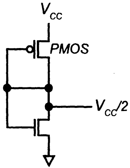
Memory capacitor in DRAM is biased to VCC/2, and the digitlines are always equilibrated and biased to VCC/2 between array accesses. Therefore, DVC2 voltage refers to a voltage level at half the level of the DC supply voltage. In most DRAM designs, the cellplate and digitline bias voltages are derived from the same generator circuit. Figure 4962b shows a simple circuit, for generating VCC/2 (DVC2) voltage, which is composed of a standard CMOS inverter with the input and output terminals shorted together. With correct transistor sizing, the output voltage of this circuit can be accurately set to VCC/2 V.
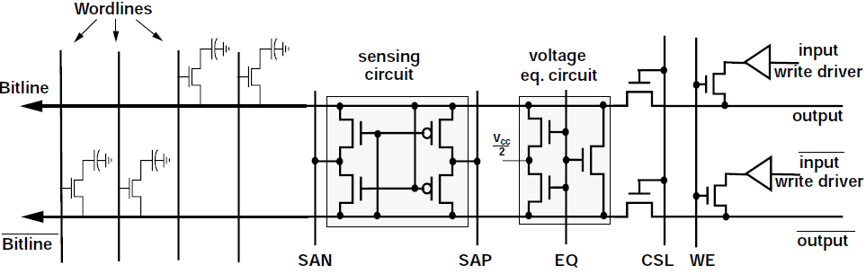
The digitlines start at VCC/2 prior to cell access and sensing. [1] Figure 4962c shows a diagram of a basic sense amplifier. More complex sense amplifiers in modern DRAM devices contain the basic elements, as well as additional circuit elements for array isolation, careful balance of the sense amplifier structure, and faster sensing capability. In Figure 4962c, the equalization (EQ) signal line controls the voltage equalization circuit. The functionality of this circuit is to ensure that the voltages on the bitline pairs are as closely matched as possible. Since the differential sense amplifier is designed to amplify the voltage differential between the bitline pairs, thus any voltage imbalance that exists on the bitline pairs prior to the activation of the access transistors would degrade the effectiveness of the sense amplifier. [2]
Figure 4962c. Diagram of a basic sense amplifier. [2]
[1] N. C.-C. Lu and H. H. Chao, Half-VDD/Bit-Line Sensing Scheme in CMOS DRAMs, IEEE Journal of Solid-State Circuits, SC19, 451, 1984.
|
||||||||
| ================================================================================= | ||||||||
|
|
||||||||