=================================================================================
Table 4233a compares the recognition rate of each defect pattern and average accuracy with classical wafer map inspection algorithms.
| Table 4233a. Comparison with classical wafer map inspection algorithms based on WM-811K wafer dataset (accuracy: %). |
| Model |
None |
Edge-Ring |
Edge-Local |
Center |
Local |
Scratch |
Random |
Donut |
Near-Full |
Average |
Ref |
| WMFPR |
95.7 |
79.7 |
85.1 |
84.9 |
68.5 |
82.4 |
79.8 |
74 |
97.9 |
83.1 |
[1] |
| DTE-WMFPR |
100 |
86.8 |
83.5 |
95.8 |
83.5 |
86 |
95.8 |
92.3 |
N/A |
90.5 |
[2] |
| WMDPI |
97.9 |
97.9 |
81.8 |
92.5 |
83.9 |
81.4 |
95.8 |
91.5 |
93.3 |
90.7 |
[3] |
| T-DenseNet |
85.5 |
66.8 |
81.5 |
64.5 |
100 |
72.6 |
65.5 |
91.2 |
99.3 |
80.8 |
[4] |
| DCNN |
98.6 |
97.6 |
92 |
97.6 |
86.7 |
93.6 |
96.7 |
96.4 |
100 |
95.5 |
[5] |
| Pre-trained CNN |
|
98.5 |
87 |
97 |
85.4 |
85.5 |
90 |
100 |
100 |
92.9 |
[6] |
| SMV |
95.7 |
79.7 |
85.1 |
84.9 |
68.5 |
82.4 |
79.8 |
74.0 |
97.9 |
83.1 |
[9] |
| CNN |
97.9 |
96.8 |
85.2 |
94.0 |
72.7 |
87.6 |
94.9 |
97.1 |
99.3 |
91.7 |
[9] |
| LR |
|
|
|
|
|
|
|
|
|
95.06 |
[17] |
| RF |
|
|
|
|
|
|
|
|
|
94.42 |
[17] |
| GBM |
|
|
|
|
|
|
|
|
|
95.35 |
[17] |
| ANN |
|
|
|
|
|
|
|
|
|
95.25 |
[17] |
| CNN |
|
|
|
|
|
|
|
|
|
89.80 |
[17] |
| LeNet |
|
|
|
|
|
|
|
|
|
96.94 |
[17] |
| MVE |
97.95 |
97.56 |
78.75 |
89.79 |
85.65 |
79.41 |
96.15 |
87.37 |
96.55 |
95.74 |
[17] |
| SVE |
97.93 |
97.94 |
81.80 |
92.54 |
83.91 |
81.36 |
95.78 |
91.49 |
93.33 |
95.87 |
[17] |
| ECNN |
98.83 |
99.22 |
94.31 |
98.85 |
93.53 |
96.73 |
96.41 |
87.60 |
100.00 |
98.57 |
[17] |
| AlexNet |
|
|
|
|
|
|
|
|
|
97.75 |
[17] |
| GoogleNet |
|
|
|
|
|
|
|
|
|
97.35 |
[17] |
| Average |
96.6 |
90.8 |
85.1 |
90.2 |
82.9 |
84.5 |
89.7 |
89.4 |
97.8 |
|
|
| Table 4233b. Comparison of balanced accuracy for WM-811K dataset between supervised learning methods and semi-supervised
learning methods. [7] |
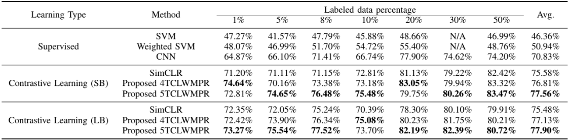
Table 4233c. Some research related to the WM-811K dataset.
| Model |
Channel |
Resolution
size |
Training
samples |
Test
samples |
Overall
accuracy |
Reference |
| DCNN |
RBG |
[26, 26, 3] |
12730 |
705 |
99.29% |
[10] |
| PCACAE |
Grayscale |
[96, 96, 1] |
13451 |
4483 |
97.27% |
[11] |
| GAN-CNN |
Grayscale |
[64, 64, 1] |
8160 |
1000 |
98.30% |
[12] |
| CNN-ECOC-SVM |
Grayscale |
[256, 256, 1] |
18000 |
2000 |
98.43% |
[13] |
| DMC1 |
RBG |
[64, 64, 3] |
103770 |
51885 |
97.01% |
[14] |
| VGG-19 |
Grayscale |
[96, 96, 1] |
11760 |
9471 |
84.81% |
[15] |
| ResNet-34 |
Grayscale |
[96, 96, 1] |
11760 |
9471 |
81.91% |
[15] |
| ResNet-50 |
Grayscale |
[96, 96, 1] |
11760 |
9471 |
87.84% |
[15] |
| MobileNetV2 |
Grayscale |
[96, 96, 1] |
11760 |
9471 |
85.39% |
[15] |
| T-DenseNet |
Grayscale |
[224, 224, 1] |
7112 |
2000 |
87.70% |
[16] |
Figure 4233a shows classification performance of some models.
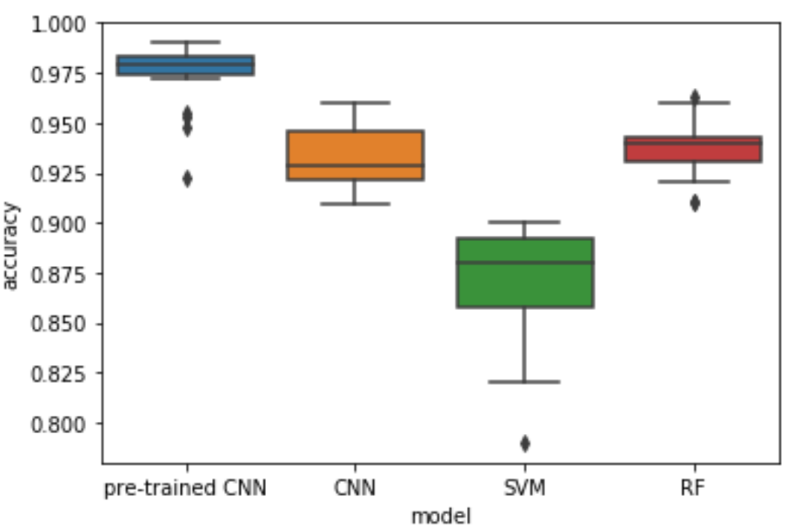
Figure 4233a. Classification performance of some models. [6]
In Figure 4233b, these experiments took only 10% of the WM-811K data
and added different levels of noise to observe the tendency of
accuracy. It can be seen that the 10% data declining accuracy
is quite similar to the declining accuracy calculated from 100% data. According to the results, the user can try to estimate how much the noise influences the accuracy by using a small amount of existing data if we do not know the
distribution of unknown data.
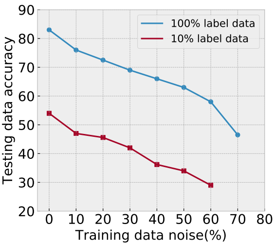
| Figure 4233b. The tendency of accuracy on different levels
of noise. It shows that the two descending curves are very
similar under different percentages of data. [8] |
============================================
[1] Wu, M.-J.; Jang, J.-S.; Chen, J.-L. Wafer map failure pattern recognition and similarity ranking for large-scale data sets. IEEE Trans.
Semicond. Manuf. 2015, 28, 1–12.
[2] Piao, M.; Jin, C.H.; Lee, J.Y.; Byun, J.-Y. Decision tree ensemble-based wafer map failure pattern recognition based on radon
transform-based features. IEEE Trans. Semicond. Manuf. 2018, 31, 250–257.
[3] Saqlain, M.; Jargalsaikhan, B.; Lee, J.Y. A voting ensemble classifier for wafer map defect patterns identification in semiconductor
manufacturing. IEEE Trans. Semicond. Manuf. 2019, 32, 171–182.
[4] Shen, Z.; Yu, J. Wafer map defect recognition based on deep transfer learning. In Proceedings of the 2019 IEEE International
Conference on Industrial Engineering and Engineering Management, Macao, China, 15–18 December 2019.
[5] Qiao Xu, Naigong Yu and Firdaous Essaf, Improved Wafer Map Inspection Using Attention Mechanism and Cosine Normalization, Machines, https://doi.org/10.3390/machines10020146, 10, 146, 2022.
[6] Yunseon Byun and Jun-Geol Baek, Mixed Pattern Recognition Methodology on Wafer Maps with Pre-trained Convolutional Neural Networks, 2022.
[7] Hanbin Hu, Chen He and Peng Li, Semi-supervised Wafer Map Pattern Recognition using Domain-Specific Data Augmentation and Contrastive Learning, DOI: 10.1109/ITC50571.2021.00019, 2021 IEEE International Test Conference (ITC), 2021.
[8] Song-Bo Yang and Tian-li Yu, Pseudo-Representation Labeling Semi-Supervised Learning, https://doi.org/10.48550/arXiv.2006.00429, 2020.
[9] Roberto di Bella, Diego Carrera, Beatrice Rossi, Pasqualina Fragneto and Giacomo Boracchi, Wafer Defect Map Classification Using Sparse Convolutional Networks, International Conference on Image Analysis and Processing, Image Analysis and Processing – ICIAP 2019 pp 125–136.
[10] Ashadullah Shawon, Md Omar Faruk, Masrur Bin Habib, Abdullah Mohammad Khan, Silicon Wafer Map Defect Classification Using Deep Convolutional Neural Network With Data Augmentation, 2019 IEEE 5th International Conference on Computer and Communications (ICCC 2019).
[11] Yu J, Liu J. Two-dimensional principal component analysis-based convolutional autoencoder for wafer map defect detection. IEEE Trans
Ind Electron. 2021;68(9):8789-8797.
[12] Ji Y, Lee JH, Using GAN to improve CNN performance of wafer map defect type classification: yield enhancement. In: 2020 31st Annual
SEMI Advanced Semiconductor Manufacturing Conference (ASMC). Saratoga Springs, NY, USA, 2020:1-6.
[13] Jin CH, Kim HJ, Piao Y, Li M, Piao M. Wafer map defect pattern classification based on convolutional neural network features and error-
correcting output codes. J Intell Manuf. 2020;31(8):1861-1875.
[14] Tsai TH, Lee YC. A light-weight neural network for wafer map classification based on data augmentation. IEEE Trans Semicond Manuf.
2020;33(4):663-672.
[15] Maksim K, Kirill B, Eduard Z, et al. classification of wafer maps defect based on deep learning methods with small amount of data. In:
2019 International Conference on Engineering and Telecommunication (EnT). Dolgoprudny, Russia, 2019:1-5.
[16] Shen Z, Yu J, Wafer map defect recognition based on deep transfer learning. In: 2019 IEEE International Conference on Industrial Engineering and Engineering Management (IEEM). Macao, China, 2019:1568-1572.
[17] Chia-Yu Hsu and Ju-Chien Chien, Ensemble convolutional neural networks with weighted majority for wafer bin map pattern classification, Journal of Intelligent Manufacturing, https://doi.org/10.1007/s10845-020-01687-7, 2020.
|